LC资料下载.pdf
《LC资料下载.pdf》由会员分享,可在线阅读,更多相关《LC资料下载.pdf(12页珍藏版)》请在冰点文库上搜索。
-40Cto+85C-Automotive(E):
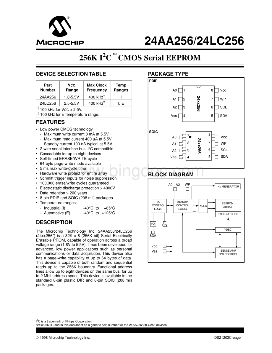
-40Cto+125CA0A1A2VssVccWPSCLSDA1234876524xx256PDIPA0A1A2VSSVCCWPSCLSDA24xx25612348765SOICHVGENERATOREEPROMARRAYPAGELATCHESYDECXDECSENSEAMPR/WCONTROLMEMORYCONTROLLOGICI/OCONTROLLOGICA0A2SDASCLVCCVSSWPI/O256KI2CCMOSSerialEEPROMI2CisatrademarkofPhilipsCorporation.*24xx256isusedinthisdocumentasagenericpartnumberforthe24AA256/24LC256devices.24AA256/24LC256DS21203C-page21998MicrochipTechnologyInc.1.0ELECTRICALCHARACTERISTICS1.1MaximumRatings*VCC.7.0VAllinputsandoutputsw.r.t.VSS.-0.6VtoVCC+1.0VStoragetemperature.-65Cto+150CAmbienttemp.withpowerapplied.-65Cto+125CSolderingtemperatureofleads(10seconds).+300CESDprotectiononallpins.4kV*Notice:
Stressesabovethoselistedunder“MaximumRatings”maycausepermanentdamagetothedevice.Thisisastressratingonlyandfunctionaloperationofthedeviceatthoseoranyotherconditionsabovethoseindicatedintheoperationallistingsofthisspecificationisnotimplied.Exposuretomaximumratingconditionsforextendedperi-odsmayaffectdevicereliability.TABLE1-1PINFUNCTIONTABLEFIGURE1-1:
BUSTIMINGDATANameFunctionA0,A1,A2UserConfigurableChipSelectsVSSGroundSDASerialDataSCLSerialClockWPWriteProtectInputVCC+1.8to5.5V(24AA256)+2.5to5.5V(24LC256)TABLE1-2DCCHARACTERISTICSAllparametersapplyacrossthespecifiedoperatingrangesunlessotherwisenoted.Industrial(I):
VCC=+1.8Vto5.5VTamb=-40Cto+85CAutomotive(E):
VCC=+4.5Vto5.5VTamb=-40Cto125CParameterSymbolMinMaxUnitsConditionsA0,A1,A2,SCL,SDA,andWPpins:
HighlevelinputvoltageVIH0.7VCCVLowlevelinputvoltageVIL0.3VCC0.2VCCVVVcc2.5VVcc2.5VHysteresisofSchmittTriggerinputs(SDA,SCLpins)VHYS0.05VCCVVCC2.5V(Note)LowleveloutputvoltageVOL0.40VIOL=3.0mAVCC=4.5VIOL=2.1mAVCC=2.5VInputleakagecurrentILI-1010AVIN=VSSorVCC,WP=VSSVIN=VSSorVCC,WP=VCCOutputleakagecurrentILO-1010AVOUT=VSSorVCCPincapacitance(allinputs/outputs)CIN,COUT10pFVCC=5.0V(Note)Tamb=25C,fc=1MHzOperatingcurrentICCWrite3mAVCC=5.5VICCRead400AVCC=5.5V,SCL=400kHzStandbycurrentICCS1ASCL=SDA=VCC=5.5VA0,A1,A2,WP=VSSNote:
Thisparameterisperiodicallysampledandnot100%tested.WP(unprotected)(protected)TSU:
WPTHD:
WPSCLSDAINTSU:
STASDAOUTTHD:
STATLOWTHIGHTRTBUFTAATHD:
DATTSU:
STOTSPTFVHYS1998MicrochipTechnologyInc.DS21203C-page324AA256/24LC256TABLE1-3ACCHARACTERISTICSAllparametersapplyacrossthespec-ifiedoperatingrangesunlessother-wisenoted.Industrial(I):
VCC=+4.5Vto5.5VTamb=-40Cto125CParameterSymbolMinMaxUnitsConditionsClockfrequencyFCLK100100400kHz4.5VVCC5.5V(ETemprange)1.8VVCC2.5V2.5VVCC5.5VClockhightimeTHIGH40004000600ns4.5VVCC5.5V(ETemprange)1.8VVCC2.5V2.5VVCC5.5VClocklowtimeTLOW470047001300ns4.5VVCC5.5V(ETemprange)1.8VVCC2.5V2.5VVCC5.5VSDAandSCLrisetime(Note1)TR10001000300ns4.5VVCC5.5V(ETemprange)1.8VVCC2.5V2.5VVCC5.5VSDAandSCLfalltimeTF300ns(Note1)STARTconditionholdtimeTHD:
STA40004000600ns4.5VVCC5.5V(ETemprange)1.8VVCC2.5V2.5VVCC5.5VSTARTconditionsetuptimeTSU:
STA47004700600ns4.5VVCC5.5V(ETemprange)1.8VVCC2.5V2.5VVCC5.5VDatainputholdtimeTHD:
DAT0ns(Note2)DatainputsetuptimeTSU:
DAT250250100ns4.5VVCC5.5V(ETemprange)1.8VVCC2.5V2.5VVCC5.5VSTOPconditionsetuptimeTSU:
STO40004000600ns4.5VVCC5.5V(ETemprange)1.8VVCC2.5V2.5VVCC5.5VWPsetuptimeTSU:
WP40004000600ns4.5VVCC5.5V(ETemprange)1.8VVCC2.5V2.5VVCC5.5VWPholdtimeTHD:
WP470047001300ns4.5VVCC5.5V(ETemprange)1.8VVCC2.5V2.5VVCC5.5VOutputvalidfromclock(Note2)TAA35003500900ns4.5VVCC5.5V(ETemprange)1.8VVCC2.5V2.5VVCC5.5VBusfreetime:
TimethebusmustbefreebeforeanewtransmissioncanstartTBUF470047001300ns4.5VVCC5.5V(ETemprange)1.8VVCC2.5V2.5VVCC5.5VOutputfalltimefromVIHminimumtoVILmaximumTOF10250nsCB100pF(Note1)Inputfilterspikesuppression(SDAandSCLpins)TSP50ns(Notes1and3)Writecycletime(byteorpage)TWC5msEndurance100,000cycles25C,VCC=5.0V,BlockMode(Note4)Note1:
Not100%tested.CB=totalcapacitanceofonebuslineinpF.2:
Asatransmitter,thedevicemustprovideaninternalminimumdelaytimetobridgetheundefinedregion(minimum300ns)ofthefallingedgeofSCLtoavoidunintendedgenerationofSTARTorSTOPconditions.3:
ThecombinedTSPandVHYSspecificationsareduetonewSchmitttriggerinputswhichprovideimprovednoisespikesuppression.ThiseliminatestheneedforaTIspecificationforstandardoperation.4:
Thisparameterisnottestedbutguaranteedbycharacterization.Forenduranceestimatesinaspecificapplication,pleaseconsulttheTotalEnduranceModelwhichcanbeobtainedonMicrochipsBBSorwebsite.24AA256/24LC256DS21203C-page41998MicrochipTechnologyInc.2.0PINDESCRIPTIONS2.1A0,A1,A2ChipAddressInputsTheA0,A1,A2inputsareusedbythe24xx256formultipledeviceoperation.Thelevelsontheseinputsarecomparedwiththecorrespondingbitsintheslaveaddress.Thechipisselectedifthecompareistrue.Uptoeightdevicesmaybeconnectedtothesamebusbyusingdifferentchipselectbitcombinations.Ifleftunconnected,theseinputswillbepulleddowninternallytoVSS.2.2SDASerialDataThisisabi-directionalpinusedtotransferaddressesanddataintoanddataoutofthedevice.Itisanopen-drainterminal,therefore,theSDAbusrequiresapull-upresistortoVCC(typical10kfor100kHz,2kfor400kHz)FornormaldatatransferSDAisallowedtochangeonlyduringSCLlow.ChangesduringSCLhigharereservedforindicatingtheSTARTandSTOPconditions.2.3SCLSerialClockThisinputisusedtosynchronizethedatatransferfromandtothedevice.2.4WPThispincanbeconnectedtoeitherVSS,VCCorleftfloating.Aninternalpull-downonthispinwillkeepthedeviceintheunprotectedstateifleftfloating.IftiedtoVSSorleftfloating,normalmemoryoperationisenabled(read/writetheentirememory0000-7FFF).IftiedtoVCC,WRITEoperationsareinhibited.Readoperationsarenotaffected.3.0FUNCTIONALDESCRIPTIONThe24xx256supportsabi-directional2-wirebusanddatatransmissionprotocol.Adevicethatsendsdataontothebusisdefinedasatransmitter,andadevicereceivingdataasareceiver.Thebusmustbecon-trolledbyamasterdevicewhichgeneratestheserialclock(SCL),controlsthebusaccess,andgeneratestheSTARTandSTOPconditionswhilethe24xx256worksasaslave.Bothmasterandslavecanoperateasatransmitterorreceiver,butthemasterdevicedeter-mineswhichmodeisactivated.4.0BUSCHARACTERISTICSThefollowingbusprotocolhasbeendefined:
Datatransfermaybeinitiatedonlywhenthebusisnotbusy.Duringdatatransfer,thedatalinemustremainstablewhenevertheclocklineisHIGH.ChangesinthedatalinewhiletheclocklineisHIGHwillbeinterpretedasaSTARTorSTOPcondition.Accordingly,thefollowingbusconditionshavebeendefined(Figure4-1).4.1BusnotBusy(A)BothdataandclocklinesremainHIGH.4.2StartDataTransfer(B)AHIGHtoLOWtransitionoftheSDAlinewhiletheclock(SCL)isHIGHdeterminesaSTARTcondition.AllcommandsmustbeprecededbyaSTARTcondition.4.3StopDataTransfer(C)ALOWtoHIGHtransitionoftheSDAlinewhiletheclock(SCL)isHIGHdeterminesaSTOPcondition.AlloperationsmustendwithaSTOPcondition.4.4DataValid(D)Thestateofthedatalinerepresentsvaliddatawhen,afteraSTARTcondition,thedatalineisstableforthedurationoftheHIGHperiodoftheclocksignal.ThedataonthelinemustbechangedduringtheLOWperiodoftheclocksignal.Thereisonebitofdataperclockpulse.EachdatatransferisinitiatedwithaSTARTconditionandterminatedwithaSTOPcondition.ThenumberofthedatabytestransferredbetweentheSTARTandSTOPconditionsisdeterminedbythemasterdevice.4.5AcknowledgeEachreceivingdevice,whenaddressed,isobligedtogenerateanacknowledgesignalafterthereceptionofeachbyte.Themasterdevicemustgenerateanextraclockpulsewhichisassociatedwiththisacknowledgebit.AdevicethatacknowledgesmustpulldowntheSDAlineduringtheacknowledgeclockpulseinsuchawaythattheSDAlineisstableLOWduringtheHIGHperiodoftheacknowledgerelatedclockpulse.Ofcourse,setupandholdtimesmustbetakenintoaccount.Dur-ingreads,amastermustsignalanendofdatatotheslavebyNOTgeneratinganack
 升级会员
升级会员 